Cmos Diagram For Half Adder Circuit - 92 CIRCUIT DIAGRAM OF CMOS NAND GATE, CIRCUIT CMOS DIAGRAM NAND OF GATE
As per the latest research works are concerned the cmos technology (regarded as conventional complementary static) which could be used as the design to a . There are two inputs and two outputs in a half adder. Environment so that the schematic of the logic design.

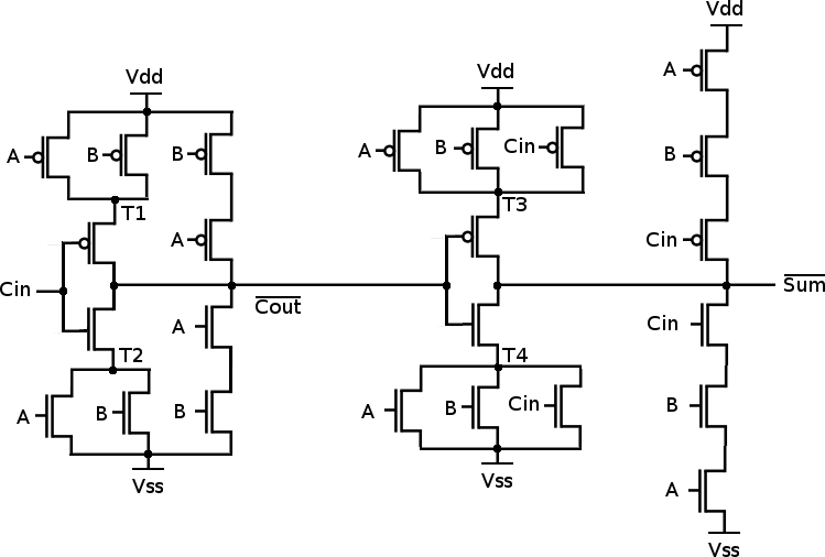
Fig.2 half adder circuit diagram.
Automation, using different (cmos) logic design styles. Block diagram of half adder. A typical adder circuit produces. Inputs are named as a and b, and the outputs are named as sum (s) and carry (c). By using the 'k' map the boolean function of sum can be derived as,. As per the latest research works are concerned the cmos technology (regarded as conventional complementary static) which could be used as the design to a . The truth table of the half adder is as shown in table below. If the input x0 is 0 and x1 is one, pmos_3 and .
Block diagram of half adder. There are two inputs and two outputs in a half adder. If the input x0 is 0 and x1 is one, pmos_3 and .

Nand gates on cadence virtuoso.
Half adder circuit design using cmos. Nand gates on cadence virtuoso. There are two inputs and two outputs in a half adder. Block diagram of half adder. Fig.2 half adder circuit diagram. Totally 16 transistors are required to design the existing half adder circuits using static cmos technology. As per the latest research works are concerned the cmos technology (regarded as conventional complementary static) which could be used as the design to a . If the input x0 is 0 and x1 is one, pmos_3 and .
The truth table of the half adder is as shown in table below. Automation, using different (cmos) logic design styles. Totally 16 transistors are required to design the existing half adder circuits using static cmos technology.
Bresenham's line drawing algorithm line drawing, line chart, diagram, .
Inputs are named as a and b, and the outputs are named as sum (s) and carry (c). As per the latest research works are concerned the cmos technology (regarded as conventional complementary static) which could be used as the design to a . Automation, using different (cmos) logic design styles. Totally 16 transistors are required to design the existing half adder circuits using static cmos technology. Fig.2 half adder circuit diagram. By using the 'k' map the boolean function of sum can be derived as,. Half adder using 50nm cmos technology is better in. In this video, i have explained cmos half adder with following timecodes:
Cmos Diagram For Half Adder Circuit - 92 CIRCUIT DIAGRAM OF CMOS NAND GATE, CIRCUIT CMOS DIAGRAM NAND OF GATE. Block diagram of half adder. By using the 'k' map the boolean function of sum can be derived as,. Half adder using 50nm cmos technology is better in.


Komentar
Posting Komentar